热点文献带您关注半导体领域的最新进展——图书馆前沿文献专题推荐服务(80)
2023-06-12
在上一期热点文献推荐中,我们为您推荐了人工智能领域的最新发展前沿,包括使用AlphaCode生成竞争级别的代码、可穿戴式心脏超声成像仪、用于自动驾驶汽车安全验证的密集强化学习、用于深度学习建模的肌电数字孪生。
本期我们为您选取了4篇文献,介绍半导体领域的最新发展前沿,包括用于太赫兹应用的电子元器件、用于深度学习加速器的CMOS兼容电化学突触晶体管阵列、用于晶圆级可拉伸电子器件的真空沉积聚合物电介质、使用粘附光刻的过渡金属二硫族化合物场效应晶体管的晶圆级集成。

Electronic metadevices for terahertz applications
Nikoo, Mohammad Samizadeh, etc.
NATURE, 2023, 614(7948): 451–455
The evolution of electronics has largely relied on downscaling to meet the continuous needs for faster and highly integrated devices. As the channel length is reduced, however, classic electronic devices face fundamental issues that hinder exploiting materials to their full potential and, ultimately, further miniaturization. For example, the carrier injection through tunnelling junctions dominates the channel resistance, whereas the high parasitic capacitances drastically limit the maximum operating frequency. In addition, these ultra-scaled devices can only hold a few volts due to the extremely high electric fields, which limits their maximum delivered power. Here we challenge such traditional limitations and propose the concept of electronic metadevices, in which the microscopic manipulation of radiofrequency fields results in extraordinary electronic properties. The devices operate on the basis of electrostatic control of collective electromagnetic interactions at deep subwavelength scales, as an alternative to controlling the flow of electrons in traditional devices, such as diodes and transistors. This enables a new class of electronic devices with cutoff frequency figure-of-merit well beyond ten terahertz, record high conductance values, extremely high breakdown voltages and picosecond switching speeds. This work sets the stage for the next generation of ultrafast semiconductor devices and presents a new paradigm that potentially bridges the gap between electronics and optics.
阅读原文:https://www.nature.com/articles/s41586-022-05595-z
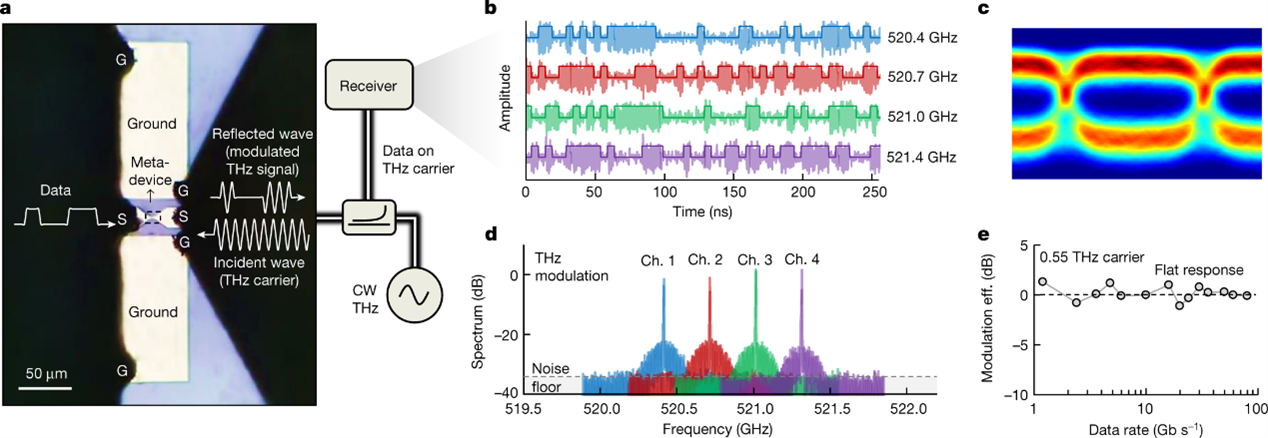
High-performance THz data transmitters using electronic metadevices

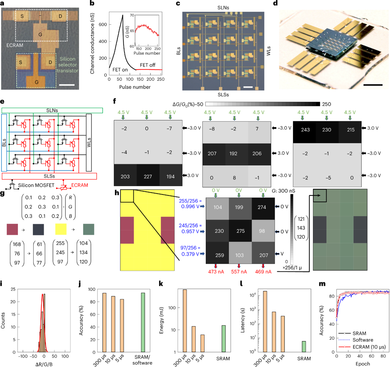
CMOS-compatible electrochemical synaptic transistor arrays for deep learning accelerators
Cui, Jinsong, etc.
NATURE ELECTRONICS, 2023, 6: 292–300
In-memory computing architectures based on memristive crossbar arrays could offer higher computing efficiency than traditional hardware in deep learning applications. However, the core memory devices must be capable of performing high-speed and symmetric analogue programming with small variability. They should also be compatible with silicon technology and scalable to nanometre-sized footprints. Here we report an electrochemical synaptic transistor that operates by shuffling protons between a hydrogenated tungsten oxide channel and gate through a zirconium dioxide protonic electrolyte. These devices offer multistate and symmetric programming of channel conductance via gate-voltage pulse control and small cycle-to-cycle variation. They can be programmed at frequencies approaching the megahertz range and exhibit endurances of over 100 million read-write cycles. They are also compatible with complementary metal-oxide-semiconductor technology and can be scaled to lateral dimensions of 150 x 150 nm2. Through monolithic integration with silicon transistors, we show that pseudo-crossbar arrays can be created for area- and energy-efficient deep learning accelerator applications.
Oxide-based solid-state protonic electrochemical transistors that have symmetric operation and are compatible with CMOS technology can be used to create crossbar arrays for deep learning applications.
阅读原文:https://www.nature.com/articles/s41928-023-00939-7
Monolithic integration of protonic ECRAMs with silicon transistors

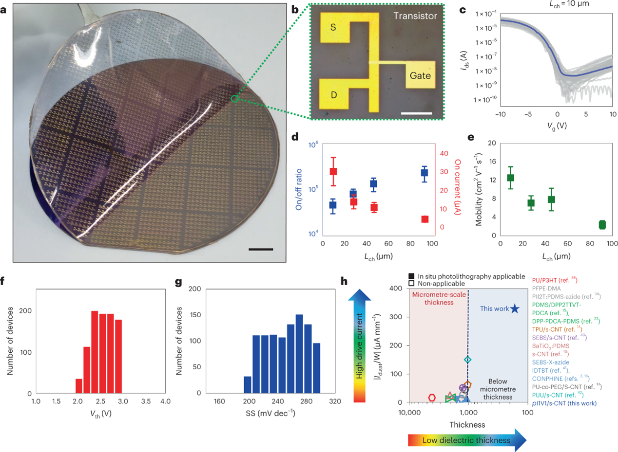
A vacuum-deposited polymer dielectric for wafer-scale stretchable electronics
Koo, Ja Hoon, etc.
NATURE ELECTRONICS, 2023, 6(2): 137–145
A thin and stretchable polymer layer can be fabricated over large areas with high uniformity using a vacuum-deposition method and used as the gate dielectric in stretchy carbon-nanotube-based transistors and circuits that can function at 40% strain.
Despite recent advances in materials and fabrication technologies, the development of intrinsically stretchable electronic devices with large-area uniformity, low power consumption and performance comparable with conventional rigid devices remains challenging. A key limitation is the absence of an elastic dielectric material that can be thin and uniform over large areas as well as offer robust insulating properties and high mechanical and chemical stability. Here we show that a vacuum-deposited elastic polymer layer can be used as the gate dielectric in stretchy field-effect transistors with carbon nanotube channels and microcracked gold electrodes. The polymer dielectric layer has high insulation properties (at a thickness below 200 nm), high stability and large-area uniformity. An 8-inch wafer array of the stretchable carbon nanotube transistors exhibits good uniformity in their electrical performance and can maintain their performance after 1,000 stretching cycles at 40% strain. We use the transistors to construct stretchy inverters and logic gates that can function under applied strains of up to 40%.
阅读原文:https://www.nature.com/articles/s41928-023-00918-y
Intrinsically stretchable CNT transistors using a vacuum-deposited dielectric film

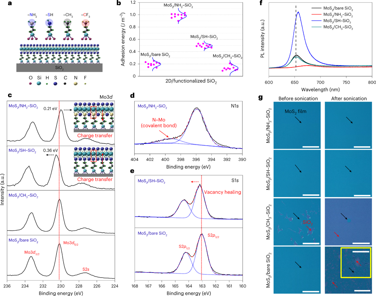
Wafer-scale integration of transition metal dichalcogenide field-effect transistors using adhesion lithography
Nguyen, Van Luan, etc.
NATURE ELECTRONICS, 2023, 6(2): 146–153
Field-effect transistors based on two-dimensional materials are a potential replacement for silicon-based devices in next-generation semiconductor chips. However, the weak interfacial adhesion energy between two-dimensional materials and substrates can lead to low yields and non-uniform transistors on the wafer scale. Furthermore, conventional photolithography processes-including photochemical reactions and chemical etching-can damage atomically thin materials. Here we show that the interfacial adhesion energy between two-dimensional materials and different substrates can be quantified using a four-point bending method. We find that a molybdenum disulfide/silicon dioxide interface has an interfacial adhesion energy of 0.2 J m-2, which can be modulated from 0 to 1.0 J m-2 by incorporating self-assembled monolayers with different end-termination chemistries. We use this to create an adhesion lithography method that is based on adhesion energy differences and physical etching processes. We use this approach to fabricate more than 10,000 molybdenum disulfide field-effect transistors on six-inch wafers with a yield of around 100%.
阅读原文:https://www.nature.com/articles/s41928-022-00890-z
Engineering the adhesion energy of MoS2/insulator interface with various SAMs
“前沿文献专题推荐服务”是图书馆情报服务部学科服务的重要内容。欢迎有相关需求的科研人员与我们联系,我们将为您提供更有针对性的定题服务。
联系电话:62281933 62283502
地址:西土城校区图书馆125室情报服务部
联系人:杨老师 闫老师
邮箱:yandong80@bupt.edu.cn
往期精彩推荐
热点文献带您关注AI领域的最新进展——图书馆前沿文献专题推荐服务(79)
热点文献带您关注通信领域的最新进展——图书馆前沿文献专题推荐服务(78)
热点文献带您关注半导体领域的最新进展——图书馆前沿文献专题推荐服务(77)
热点文献带您关注AI Transformer的最新进展——图书馆前沿文献专题推荐服务(76)
热点文献带您关注低轨卫星通信技术的最新进展——图书馆前沿文献专题推荐服务(75)
热点文献带您关注惯性测量单元的最新进展——图书馆前沿文献专题推荐服务(74)
热点文献带您关注存算一体技术的最新进展——图书馆前沿文献专题推荐服务(73)
热点文献带您关注电子皮肤的最新进展——图书馆前沿文献专题推荐服务(72)
热点文献带您关注AI的最新进展——图书馆前沿文献专题推荐服务(71)
热点论文带您探索未来网络中使用的新材料以及相关技术 ——图书馆前沿文献专题推荐服务(70)
热点文献带您关注AI图神经网络的最新进展——图书馆前沿文献专题推荐服务(69)
热点论文带您探索新型网络架构以及超材料在未来通信中的应用——图书馆前沿文献专题推荐服务(68)
热点文献带您关注AI深度强化学习的最新进展——图书馆前沿文献专题推荐服务(67)
热点论文带您探索新型网络架构以及超表面在未来通信中的应用——图书馆前沿文献专题推荐服务(66)
热点文献带您关注AI领域的最新进展——图书馆前沿文献专题推荐服务(65)
热点论文带您领略半导体领域的最新进展——图书馆前沿文献专题推荐服务(64)
热点文献带您关注AI领域的最新进展——图书馆前沿文献专题推荐服务(63)
热点论文带您探索智能化以及超表面在未来通信中的应用——图书馆前沿文献专题推荐服务(62)
热点文献带您关注AI领域的最新进展——图书馆前沿文献专题推荐服务(61)
热点论文带您领略未来通信研究热点的最新进展——图书馆前沿文献专题推荐服务(60)
热点文献带您关注AI深度学习的最新进展——图书馆前沿文献专题推荐服务(59)
热点论文带您领略未来通信热点技术的最新进展——图书馆前沿文献专题推荐服务(58)
热点文献带您关注AI视频动作识别的最新进展——图书馆前沿文献专题推荐服务(57)
热点论文带您领略新材料半导体领域的最新进展——图书馆前沿文献专题推荐服务(56)
热点文献带您关注AI深度神经网络的最新进展——图书馆前沿文献专题推荐服务(55)
热点论文带您领略未来通信在新材料技术领域的最新进展——图书馆前沿文献专题推荐服务(54)
热点文献带您关注AI在光神经网络领域的最新进展——图书馆前沿文献专题推荐服务(53)
热点论文带您领略半导体领域的最新进展——图书馆前沿文献专题推荐服务(52)
热点文献带您关注AI在集成电路领域的最新进展——图书馆前沿文献专题推荐服务(51)
热点论文带您领略光电半导体领域的最新进展——图书馆前沿文献专题推荐服务(50)
热点文献带您关注AI与人脸识别——图书馆前沿文献专题推荐服务(49)
热点论文带您领略未来通信在新材料技术领域的最新进展——图书馆前沿文献专题推荐服务(48)
热点文献带您关注AI与生物学——图书馆前沿文献专题推荐服务(47)
热点论文带您领略未来通信在光电材料及信息编码领域的最新进展——图书馆前沿文献专题推荐服务(46)
热点文献带您关注AI与医学图像——图书馆前沿文献专题推荐服务(45)
热点论文带您领略未来通信在材料领域研究的最新进展——图书馆前沿文献专题推荐服务(44)
热点文献带您关注AI与医学研究——图书馆前沿文献专题推荐服务(43)
热点论文带您领略未来通信在海空领域研究的最新进展——图书馆前沿文献专题推荐服务(42)
热点文献带您关注AI视觉跟踪——图书馆前沿文献专题推荐服务(41)
热点论文与带您领略5G相关领域研究的最新进展——图书馆前沿文献专题推荐服务(40)
热点文献带您关注AI技术的最新进展——图书馆前沿文献专题推荐服务(39)
热点论文与带您领略5G/6G领域热点研究的最新进展——图书馆前沿文献专题推荐服务(38)
热点文献带您关注AI与边缘计算——图书馆前沿文献专题推荐服务(37)
热点论文与带您领略5G/6G基础研究的最新进展——图书馆前沿文献专题推荐服务(36)
热点文献带您关注AI强化学习——图书馆前沿文献专题推荐服务(35)
热点论文与带您领略未来通信的热点技术及最新进展——图书馆前沿文献专题推荐服务(34)
热点文献带您关注AI深度学习与计算机视觉——图书馆前沿文献专题推荐服务(33)
热点论文与带您领略5G/6G热点技术的最新进展——图书馆前沿文献专题推荐服务(32)
热点文献带您关注AI与触觉传感技术——图书馆前沿文献专题推荐服务(31)
热点论文与带您领略5G/6G热点技术的最新进展——图书馆前沿文献专题推荐服务(30)
热点文献带您关注AI与机器人——图书馆前沿文献专题推荐服务(29)
热点论文与带您领略5G/6G电子器件和太赫兹方面的最新进展——图书馆前沿文献专题推荐服务(28)
热点文献带您关注AI自动驾驶——图书馆前沿文献专题推荐服务(25)
热点论文与带您领略5G/6G通信器件材料的最新进展 ——图书馆前沿文献专题推荐服务(24)
热点文献带您关注机器学习与量子物理 ——图书馆前沿文献专题推荐服务(23)
热点论文与带您领略6G网络技术的最新发展趋势 ——图书馆前沿文献专题推荐服务(22)
热点文献带您关注模式识别——图书馆前沿文献专题推荐服务(21)
热点论文与带您领略5G/6G材料技术的最新发展——图书馆前沿文献专题推荐服务(20)
热点文献带您关注图神经网络——图书馆前沿文献专题推荐服务(19)
热点论文带您领略5G/6G的最新技术动向 ——图书馆前沿文献专题推荐服务(18)
热点文献带您关注AI主动视觉——图书馆前沿文献专题推荐服务(17)
热点论文与带您领略5G/6G的最新技术演进 ——图书馆前沿文献专题推荐服务(16)
热点文献带您关注AI计算机视觉 ——图书馆前沿文献专题推荐服务(15)
热点论文与带您领略5G/6G的硬科技与新思路 ——图书馆前沿文献专题推荐服务(14)
热点文献带您关注AI机器翻译 ——图书馆前沿文献专题推荐服务(11)
热点论文:5G/6G引领社会新进步——图书馆前沿文献专题推荐服务(10)
热点文献带您关注AI文本摘要自动生成 ——图书馆前沿文献专题推荐服务(9)
热点论文带您探究6G的无限可能——图书馆前沿文献专题推荐服务(8)
热点文献带您关注AI情感分类技术 ——图书馆前沿文献专题推荐服务(7)
热点论文带您探究5G和未来通信材料技术领域 ——图书馆前沿文献专题推荐服务(6)
前沿文献带您解读自然语言处理技术 ——图书馆前沿文献专题推荐服务(5)
热点论文带您探究5G和未来通信——图书馆前沿文献专题推荐服务 (4)
热点论文解读AI应用领域 ——图书馆前沿文献专题推荐服务(3)